Austin, April 08, 2026 (GLOBE NEWSWIRE) -- Electronic Design Automation (EDA) Market Size & Growth Insights:
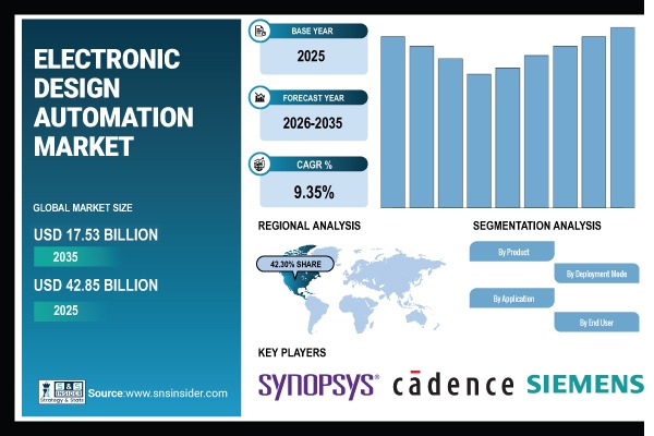
According to the SNS Insider, “The Electronic Design Automation (EDA) Market Size was valued at USD 17.53 Billion in 2025 and is projected to reach USD 42.85 Billion by 2035, growing at a CAGR of 9.35 % during 2026–2035.”
Rising Demand for Advanced Semiconductor Design and Increasing Chip Complexity to Boost Market Growth Globally
The market for electrical design automation has been driven by the need for semiconductors in a variety of industries, including consumer electronics, telecommunications, and automobiles. More AI, IoT, and 5G have all significantly increased the complexity of chip design, necessitating the usage of sophisticated EDA tools. Additionally, growing investments in semiconductor production and continuous innovation in system-on-a-chip (SoC) designs are driving industry expansion.
Get a Sample Report of Electronic Design Automation (EDA) Market Forecast @ https://www.snsinsider.com/sample-request/2102
Leading Market Players with their Product Listed in this Report are:
- Synopsys
- Cadence Design Systems
- Siemens EDA
- ANSYS
- Keysight Technologies
- Zuken
- Altair Engineering
- Autodesk
- Altium
- Mentor Graphics
- Silvaco
- AWR Corporation
- Magma Design Automation
- Dassault Systèmes
- National Instruments
- ARM Holdings
- Rambus
- Xilinx
- Intel
- Broadcom
Electronic Design Automation (EDA) Market Report Scope:
| Report Attributes | Details |
| Market Size in 2025E | USD 17.53 Billion |
| Market Size by 2035 | USD 42.85 Billion |
| CAGR | CAGR of 9.35% From 2026 to 2035 |
| Report Scope & Coverage | Market Size, Segments Analysis, Competitive Landscape, Regional Analysis, DROC & SWOT Analysis, Forecast Outlook |
| Key Segmentation | • By Product (IC Physical Design & Verification, Semiconductor IP, Computer-Aided Engineering (CAE), PCB & MCM, Services), • By Deployment Mode (Cloud-Based, On-Premises), • By Application (Memory Management Units, Microprocessors & Microcontrollers, Others), • By End User (Consumer Electronics Industry, Automotive, Healthcare) |
Purchase Single User PDF of Electronic Design Automation (EDA) Market Report (20% Discount) @ https://www.snsinsider.com/checkout/2102
Key Segmentation Analysis:
By Product
In 2025, IC Physical Design & Verification dominated with 37% share owing the growing complexity of the designs of integrated Circuit (IC), is the IC Physical Design & Verification segment which demands high accuracy. Semiconductor IP fastest growing segment during 2026–2035 as the demand for reusable units increases with bottle neck reduction and meets the demand for production-ready designs with less design cycle time and at lower development costs.
By Deployment Mode
In 2025, On-Premises dominated with 58% share owing to greater security, control, and reliability for chip design processes that require greater data confidentiality. The Public Cloud Segment is the fastest growing category, as demand for highly scalable, flexible, and cost-effective design environments continues to rise.
By Application
In 2025, Microprocessors & Microcontrollers dominated with 41% share due to their widespread use in consumer electronics, industrial system applications, and communication devices. Memory Management Units fastest growing segment during 2026–2035 due to the growing demand for high-performance computing and smart devices.
By End-User
In 2025, Consumer Electronics Industry dominated with 39% share due to high demand for smartphones, laptops, wearable devices and other smart electronics. The Automotive segment is the fastest growing segment owing to the higher adoption of electric vehicles (EVs), advanced driver-assistance systems (ADAS), and autonomous driving technologies.
Regional Insights:
In 2025, North America will account for 42.30% of the Electronic Design Automation Market. The existence of numerous top semiconductor manufacturers and EDA suppliers in the United States and Canada is responsible for a sizable portion of this dominance.
The Asia Pacific Electronic Design Automation Market is predicted to expand at a compound annual growth rate (CAGR) of 10.10% between 2026 and 2035. Due to the rapid expansion of semiconductor production in China, Taiwan, South Korea, Japan, and India, the region has been growing.
Do you have any specific queries or need any customized research on Electronic Design Automation (EDA) Market? Submit your inquiry here @ https://www.snsinsider.com/enquiry/2102
Recent Developments:
- In March 2025, Synopsys expanded its AI-driven EDA capabilities by enhancing its cloud-based design platforms to improve chip design productivity and reduce time-to-market for advanced semiconductor solutions.
- In February 2025, Cadence Design Systems introduced new AI-powered design and verification tools aimed at accelerating complex chip development and enhancing design accuracy for next-generation semiconductor applications.
Exclusive Sections of the Electronic Design Automation (EDA) Market Report (The USPs):
- EDA ADOPTION & DEPLOYMENT METRICS – helps you understand the scale of EDA tool adoption across semiconductor companies, fabless firms, and IDMs, along with deployment in advanced chip design and SoC development.
- TECHNOLOGICAL ADOPTION RATE – helps you identify the penetration of AI/ML-driven EDA tools, cloud-based design platforms, and advanced node and 3D IC design technologies.
- OPERATIONAL COST & DESIGN EFFICIENCY ANALYSIS – helps you evaluate high licensing costs, outsourcing trends, and variations in design cycle timelines based on chip complexity.
- SUPPLY CHAIN & DESIGN ECOSYSTEM INDEX – helps you assess dependency on specialized design service providers and the evolving semiconductor design ecosystem.
- REGIONAL DEMAND & MARKET INSIGHTS – helps you understand geographic adoption trends, growth in Asia-Pacific, and demand driven by AI, 5G, automotive, and high-performance computing sectors.
- COMPETITIVE LANDSCAPE – helps you gauge the competitive strength of key players in the market backed by an analysis of their technological capabilities, product offerings, market reach, and recent developments.
About Us:
SNS Insider is one of the leading market research and consulting agencies that dominates the market research industry globally. Our company's aim is to give clients the knowledge they require in order to function in changing circumstances. In order to give you current, accurate market data, consumer insights, and opinions so that you can make decisions with confidence, we employ a variety of techniques, including surveys, video talks, and focus groups around the world.
Read Other Trending Reports:
Contract Manufacturing and Design Services Market
